Blog
How to Design a Flyback Converter: Step-by-Step Guide for Engineers
How to Design a Flyback Converter: Step-by-Step Engineering Guide
How to Design a Flyback Converter: Step-by-Step Engineering Guide
📅 Updated: April 2026 | ⏱ 18 min read | 🔋 Isolated DC-DC Design
The flyback converter is arguably the most widely used isolated DC-DC topology in power electronics. From smartphone chargers and LED drivers to industrial control panels and auxiliary power supplies, its combination of simplicity, galvanic isolation, and multi-output capability makes it a go-to choice for millions of designs. In this comprehensive engineering guide, we will walk through the entire flyback converter design process: from fundamental operating principles to transformer design, component selection, snubber circuits, control loop compensation, and practical design examples.
1. What Is a Flyback Converter?
A flyback converter is a type of isolated switching power supply that stores energy in a transformer’s magnetic core during the switch-on phase and transfers it to the output when the switch turns off. Unlike a conventional transformer that transfers energy simultaneously from primary to secondary, the flyback transformer stores energy in its core and releases it alternately—technically acting more like a coupled inductor than a true transformer[reference:0].
What makes the flyback uniquely valuable:
- Galvanic isolation: Input and output are electrically isolated—essential for mains-powered supplies and safety-critical applications[reference:1].
- Multiple outputs: A single flyback transformer can have multiple secondary windings, each producing a different voltage (e.g., +5V, +12V, and -12V simultaneously)[reference:2].
- Wide input range: Handles wide input voltage variation (e.g., 85–265V AC after rectification) without topology change[reference:3].
- Low component count: Just one switch (MOSFET), one transformer, one diode, and output filter per output rail[reference:4].
- Power sweet spot: Ideal for 1W to 150W output power—beyond that, forward or full-bridge topologies are more efficient[reference:5].
💡 Key Insight: The flyback converter’s operation has two distinct phases: during tON, the MOSFET is on and energy is stored in the transformer core; during tOFF, the MOSFET turns off and the stored energy is transferred to the secondary side[reference:6].
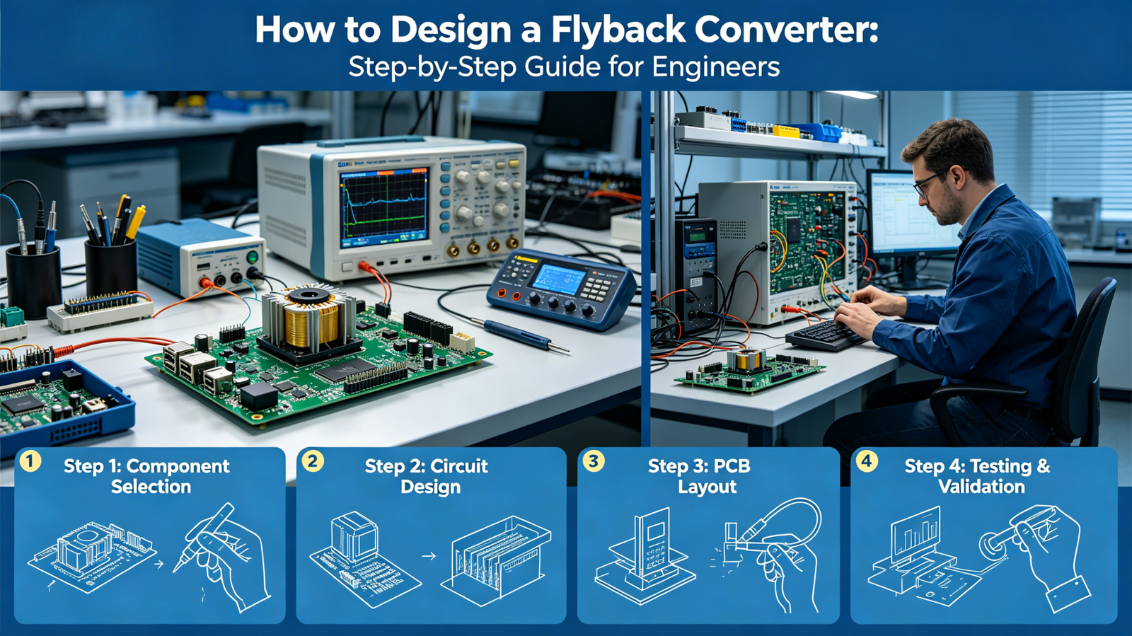
2. Step-by-Step Design Procedure
Step 1: Define Design Specifications and Operating Mode
The first step is to define the design inputs based on your application requirements:
- Input voltage range (VIN,min to VIN,max)
- Output voltage (VOUT) and output current (IOUT)
- Switching frequency (fSW) — typically 50kHz to 250kHz
- Target efficiency (η) — usually 80% to 90% for initial estimates
- Maximum duty cycle (Dmax) — often set to 0.5 (50%) for balanced design[reference:7]
You must also choose between Continuous Conduction Mode (CCM) and Discontinuous Conduction Mode (DCM). CCM is suited for medium- to high-power applications and offers lower peak currents and reduced EMI, while DCM is more compact and cost-effective for low-power, low-current applications, with lower FET and rectifier losses[reference:8]. For designs below ~30W, DCM is often preferred; above that, CCM becomes advantageous.
📐 Design Example: 12V/5A (60W) Flyback Converter
Input: 100–240V AC (rectified to ~140–340V DC)
Output: 12V / 5A (60W)
Switching frequency: 100 kHz
Operation mode: CCM
Maximum duty cycle: 0.5 at minimum input voltage[reference:9][reference:10]
Step 2: Calculate Transformer Turns Ratio
The transformer turns ratio is a critical parameter that determines voltage conversion and duty cycle. For a flyback converter operating in CCM, the relationship between duty cycle, input voltage, output voltage, and turns ratio is given by:
VOUT = (NS/NP) × VIN × D / (1 − D)
For a universal input (85-265V AC rectified to 120-375V DC) and 5V output, a typical turns ratio is around 12:1 to 15:1[reference:11]. A good practice is to set the maximum duty cycle to approximately 60% at minimum input voltage and adjust the turns ratio accordingly. The optimal turns ratio for a fixed line voltage corresponds to a duty cycle of 50%, where the converter operates most efficiently[reference:12].
For our 60W design example with VIN,min = 140V, VOUT = 12V, and Dmax = 0.5, the required turns ratio is approximately NP/NS ≈ 11.7:1[reference:13].
Step 3: Select the Transformer Core and Calculate Primary Inductance
The transformer is the most critical component. Ferrite is the most commonly used core material for flyback transformers due to its low cost, high permeability, and good high-frequency performance[reference:14].
To prevent core saturation, the volt-second product must be balanced, and the primary inductance must be properly sized. For a CCM flyback, the primary inductance can be calculated using:
LP = (VIN,min² × Dmax² × η) / (2 × POUT × fSW)
This ensures that the converter remains in CCM down to a specified minimum load (typically 20–30% of full load)[reference:15]. After determining the primary inductance and turns ratio, calculate the number of primary turns based on the core’s material properties, then derive the secondary turns[reference:16]. The core must also have sufficient window area to accommodate the required wire gauge for the expected average current[reference:17].
Step 4: Design the RCD Snubber for Leakage Inductance
Leakage inductance is an unavoidable parasitic in flyback transformers—it stores energy that cannot be transferred to the secondary. When the MOSFET turns off, this energy produces a large voltage spike across the switch, potentially 2–3× higher than the DC bus voltage. Without protection, this will destroy the MOSFET[reference:18].
The most common protection is an RCD snubber (resistor-capacitor-diode network) across the primary MOSFET. The snubber works by absorbing the leakage inductance current once the drain voltage exceeds the clamp capacitor voltage[reference:19]. The clamp voltage must be higher than the reflected output voltage to avoid continuous current through the snubber[reference:20]. A compact formula for snubber resistance is:
Rsnub = (Vclamp²) / (2 × Lleak × Ipk² × fSW)
where Vclamp is the desired clamping voltage (typically 1.2–1.5× Vreflected), Lleak is the leakage inductance, Ipk is the peak primary current, and fSW is the switching frequency[reference:21]. Increasing the clamp voltage allows a larger snubber resistance and reduces power loss, but it must remain within the MOSFET’s voltage rating.
⚠️ Critical Design Consideration: For robust design, always choose a clamp voltage that provides sufficient margin above the reflected voltage—typically 20–30% overhead. This ensures reliable operation across temperature and component tolerances[reference:22].
Step 5: Select Primary MOSFET and Secondary Rectifier Diode
The primary MOSFET must withstand the sum of the maximum DC bus voltage, the reflected output voltage, and the leakage spike voltage, plus a safety margin:
VDS,max = VIN,max + Vreflected + Vspike + margin
For a 60W flyback with 340V DC bus and a 100V reflected voltage, a 500V or 600V MOSFET is typically chosen[reference:23]. Good coupling between transformer windings is essential—leakage inductance should be kept below 1% to minimize ringing and reduce snubber losses[reference:24].
The secondary rectifier diode’s reverse voltage stress is approximately:
VD,reverse = VOUT + VIN,max × (NS/NP)
For our example, a 30A/45V Schottky diode in D²PAK package reduces forward voltage drop to 0.33V at 10A, minimizing conduction losses[reference:25]. For higher efficiency, consider using a synchronous rectification MOSFET instead of a diode, especially for low-voltage, high-current outputs.
Step 6: Design the Control Loop Compensation (TL431 + Optocoupler)
Most flyback converters use secondary-side peak current-mode control with a TL431 shunt regulator and an optocoupler to provide feedback from the secondary side to the primary-side controller[reference:26]. The output voltage is sensed and compared to the TL431’s internal 2.5V reference; any error generates a current through the optocoupler’s LED, which in turn modulates the COMP pin voltage on the primary controller.
The compensation loop has three distinct portions: the TL431 error amplifier, the optocoupler, and the controller’s internal error amplifier[reference:27]. Designing for stability requires careful selection of compensation components (Type II or Type III networks) to achieve adequate phase margin (typically >45°) and gain margin (>10dB) across all operating conditions[reference:28]. A common pitfall is neglecting the Right-Half-Plane (RHP) zero in CCM operation—the crossover frequency must be set far below the RHP zero frequency (typically less than 1/3 of the RHP zero) to ensure sufficient phase margin[reference:29].
Step 7: PCB Layout Guidelines and EMI Mitigation
Proper PCB layout is essential for flyback converter performance and reliability. Critical guidelines include:
- Minimize loop areas: Keep the primary switching loop (input capacitor → transformer primary → MOSFET → sense resistor → ground) as small as possible.
- Separate primary and secondary grounds: Maintain clear physical separation to preserve isolation and reduce common-mode noise.
- Use a ground plane: A solid ground plane on the primary side reduces inductance and improves noise immunity.
- Place the snubber close to the transformer and MOSFET: Minimizes parasitic inductance and improves clamping effectiveness.
- Add Y-capacitors across the isolation barrier: These capacitors provide a low-impedance path for common-mode currents and help meet conducted EMI limits[reference:30]. For applications requiring reinforced insulation, Y1 capacitors must be used for safety reasons[reference:31].
- Use current-compensated chokes in the input filter: Flyback converters generate both differential-mode and common-mode interference; input filtering with common-mode chokes is often necessary to meet EMI standards[reference:32].
3. Practical Design Verification
After completing the schematic and layout, thorough verification is essential:
- Transient simulation: Use SPICE-based tools (e.g., LTspice, PSpice, SIMPLIS) to simulate startup, load transients, and fault conditions before prototyping.
- Loop stability measurement: Perform gain/phase measurements using a network analyzer or the injected-signal method to verify phase margin and gain margin across load and line conditions.
- Thermal testing: Measure temperatures of the MOSFET, transformer, output diode, and snubber resistor under worst-case conditions.
- EMI pre-compliance testing: Measure conducted and radiated emissions early in the design cycle to avoid last-minute surprises.
🔧 Pro Tip: Always design with derating. Use MOSFETs rated at least 20% above calculated voltage stress, and size the snubber resistor to handle the calculated power dissipation (typically 1–3W for a 60W flyback). Leave thermal margin by adding a heatsink or airflow if needed.
4. Common Design Pitfalls and How to Avoid Them
- Transformer saturation: Always verify the volt-second balance and ensure the core does not saturate at maximum duty cycle and minimum frequency. Use a core with sufficient margin on flux density (Bmax).
- Excessive leakage inductance: Specify tight coupling between primary and secondary windings—interleaving windings can reduce leakage dramatically. Aim for leakage inductance <1% of primary inductance[reference:33].
- Loop instability: Neglecting the RHP zero in CCM designs leads to oscillation under heavy load. Set crossover frequency below 1/5 of the RHP zero frequency.
- Insufficient snubber design: Using a clamp voltage too close to the reflected voltage may cause continuous snubber conduction and overheating. Always leave 20–30% overhead[reference:34].
- Poor transformer thermal management: High-frequency operation and high current density can cause overheating. Choose a core size with adequate area product (AP) and use appropriate wire gauge (consider skin and proximity effects).
5. Conclusion
Designing a flyback converter requires careful attention to transformer design, snubber selection, component choice, and control loop compensation. By following this step-by-step methodology, engineers can create reliable, efficient, and cost-effective isolated power supplies for a wide range of applications. The flyback topology remains a workhorse of power electronics, and mastering its design is a fundamental skill for any power engineer. © 2026 Power Electronics Engineering – Your resource for flyback converter design, isolated DC-DC topology guides, and switching power supply development.